At our laboratory, we specialize in the development of advanced electronics for high-precision instrumentation, addressing the demanding requirements of scientific applications. Our work integrates expertise in analog and digital electronics, firmware development, and high-speed data transmission, with a strong focus on performance, reliability, and operation in extreme environments.
One of our key focus areas is the design of analog electronics for the readout of Silicon Photomultiplier (SiPM) sensors. These sensors are widely used in fields such as particle physics, where detecting weak light signals with high sensitivity and speed is essential. We design low-noise analog front-end electronics that operate reliably in cryogenic conditions, which impose stringent constraints on component selection, thermal behavior, and circuit performance. Through careful simulation, prototyping, and iterative testing, we ensure that our analog designs meet the highest standards of precision and stability.

In parallel, we develop digital electronics systems for data acquisition and signal processing. This includes the design of high-speed digital architectures for interfacing with analog-to-digital converters (ADCs), as well as the synchronization and timing control required for coherent data capture. A major part of our digital development involves the use of Field-Programmable Gate Arrays (FPGAs), for which we develop custom firmware using hardware description languages such as VHDL and Verilog. These FPGA-based systems enable real-time data processing, event detection, buffering, and high-throughput communication.

We also integrate microcontroller-based systems to manage control, configuration, and communication tasks within our electronic platforms. Our team develops embedded firmware, typically in C or C++, to provide robust and responsive control interfaces. These microcontrollers often interact with the FPGA logic, enabling hybrid systems that leverage the strengths of both technologies.
High-speed data transmission is critical to our systems, particularly for experiments that generate large volumes of data in real time. We implement and optimize protocols such as USB 3.0, Ethernet, and optical links to ensure reliable, low-latency transfer of information to host computers or storage systems. Our solutions are tailored to meet the specific bandwidth, latency, and environmental constraints of each application.

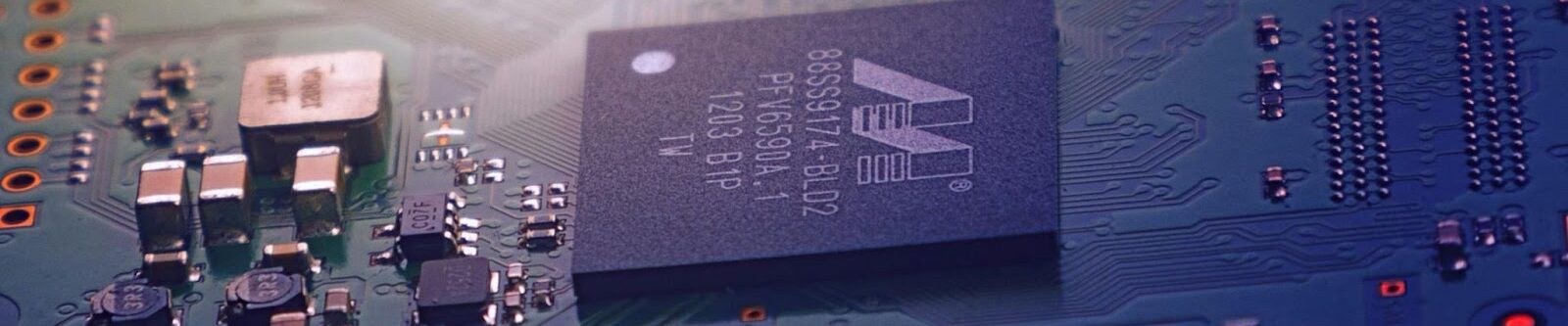
As part of the full development cycle, we also design custom printed circuit boards (PCBs), using industry-standard CAD tools. Our PCB layouts are optimized for signal integrity, power distribution, electromagnetic compatibility (EMC), and thermal performance, often requiring multi-layer designs and compact, high-density routing.

Our work is inherently collaborative, bringing together engineers, physicists, and system designers to achieve integrated solutions that meet complex experimental requirements. We participate in system-level architecture planning, provide detailed technical documentation, and support integration, testing, and deployment efforts.
